It’s easy to envisage what the term ‘printable electronics’ might mean but, until recently, the practice it described didn’t look much like the picture in anyone’s head. Now, however, Dr Aaron Franklin, associate professor of electrical and computer engineering at Duke University, and Dr Cinzia Casiraghi, professor of neuroscience at the University of Manchester, have developed the technique and materials necessary for what they call fully print-in-place flexible electronics. Medical Device Developments’ Jim Banks finds out how they’re enabling the creation of everything from personalised bandages to skin-mimicking sensors for the next generation of healthcare.
For most of us, modern electronics are synonymous with silicon, the material that began the age of information technology by enabling the mass production of reliable semiconductors at relatively low cost.
And yet, as far as silicon has taken us and as small as the transistors made from it have become, with growing demand for flexible, adaptable and compact devices, we are pushing up against its physical limitations.
Dr Aaron Franklin, associate professor of electrical and computer engineering at Duke University, has spent much of his professional life facing up to that fact. His focus is developing nanoscale alternatives to silicon for future transistor applications.
As he puts it, in his previous role at American tech firm IBM, “the question was whether we could replace silicon and breathe life into a decades-old technology”.
The answers he gave using carbon nanotube transistors, which combine atom-thin structures and strong electric conductivity, were good enough to earn him an outstanding technical achievement recognition, but there’s still some way to go before a true competitor for silicon electronics reaches the market.
Even so, since leaving IBM for Duke, Franklin has made considerable progress by zeroing in on one of silicon’s most obvious shortcomings: its lack of flexibility.
Silicon simply can’t be adapted for the same applications as the materials researchers are starting to use to 3D-print electronic devices – including thin-film transistors, capacitors and resistors – on various substrates.
“People ask me why I am pursuing printed electronics when silicon chips are relatively cheap,” he explains. “But it’s not about replacing silicon, which will always perform better.
“There are things that silicon cannot do. There are much-needed technological advances that the core silicon technology cannot deliver.”
Advances relevant to medical devices are foremost among those.
As the world moves towards a virtual and remote healthcare paradigm, print-in-place electronics could enable the fast and inexpensive creation of flexible, skin-conforming medical devices like personalised bandages, wearable sensors and even diagnostic ‘tattoos’.
The capabilities of print-in-place electronics
The concept of printed electronics is not new by any means, but Franklin is pushing for something much more advanced and recognisable – what he calls ‘print-in-place electronics’.
“I want to bridge perception and reality,” says Franklin. “When they hear about printed electronics, people expect to upload a circuit model to a 3D printer and get the whole circuit delivered a short time later.
“In fact, the fully printed circuit is usually processed further once it is printed.”
Silicon-based insulating materials are typically rigid and brittle, so their potential for creating flexible electronic circuits is severely limited.
Unhelpfully, the other materials that have been used as insulators for printed circuits have their own issues, and usually require high processing temperatures.
Often, the circuits are baked in an oven at temperatures of 100ºC or more post-printing.
“Print-in-place is the term I use to re-educate people about where we are and what needs to be done,” Franklin explains.
Specifically, there needs to be further development of inks that yield the electronic properties necessary to act as semiconductors and insulators, respectively.
Then, there are issues with compatibility, as those inks need to work together to achieve the cascade of functionality that defines a transistor.
Lastly, there are a whole set of challenges with the printing process itself, which needs to achieve higher speeds and greater throughput, like a printing press, to enable the mass production of printed circuits on a variety of flexible substrates.
“Now, we are at the stage of getting the individual inks to work,” Franklin says. “Then we can look at compatibility.
“We need parallel progress in all areas, including manufacturing, but first we need a platform of robust inks in order to look at further development.”
Transatlantic teamwork to find transistor materials
The search for that platform took a big step forward when Franklin met Cinzia Casiraghi, a professor in nanoscience at the University of Manchester, at a conference.
Upon hearing Franklin speak, Casiraghi knew that their research interests were in close alignment.
He was working on compatibility and the printing process, and he had a printing process for carbon nanotubes.
She was focused on the materials side, notably in the area of inkjet-printable 2D crystal inks for the fabrication of flexible and low-cost electronic devices.
“The biggest challenge is that there is a wide range of materials that we use but we don’t have the perfect materials for transistors,” she explains. “It is hard to find good semiconductors because their performance and stability needs to be improved.
“We also need to convince the community that we can make reproducible devices that perform to exactly the same standard every time.
“Before I met Aaron, I had developed water-based, bio-compatible inks.
“The formulation process can be applied to any material that comes in a stack of layers. We have graphene inks, semiconductor inks and hexagonal boron nitride inks that act as insulators.”
That was the perfect starting point for a collaboration. In late 2019, Casiraghi’s team developed insulating dielectric inks suitable for Franklin’s print-in-place process.
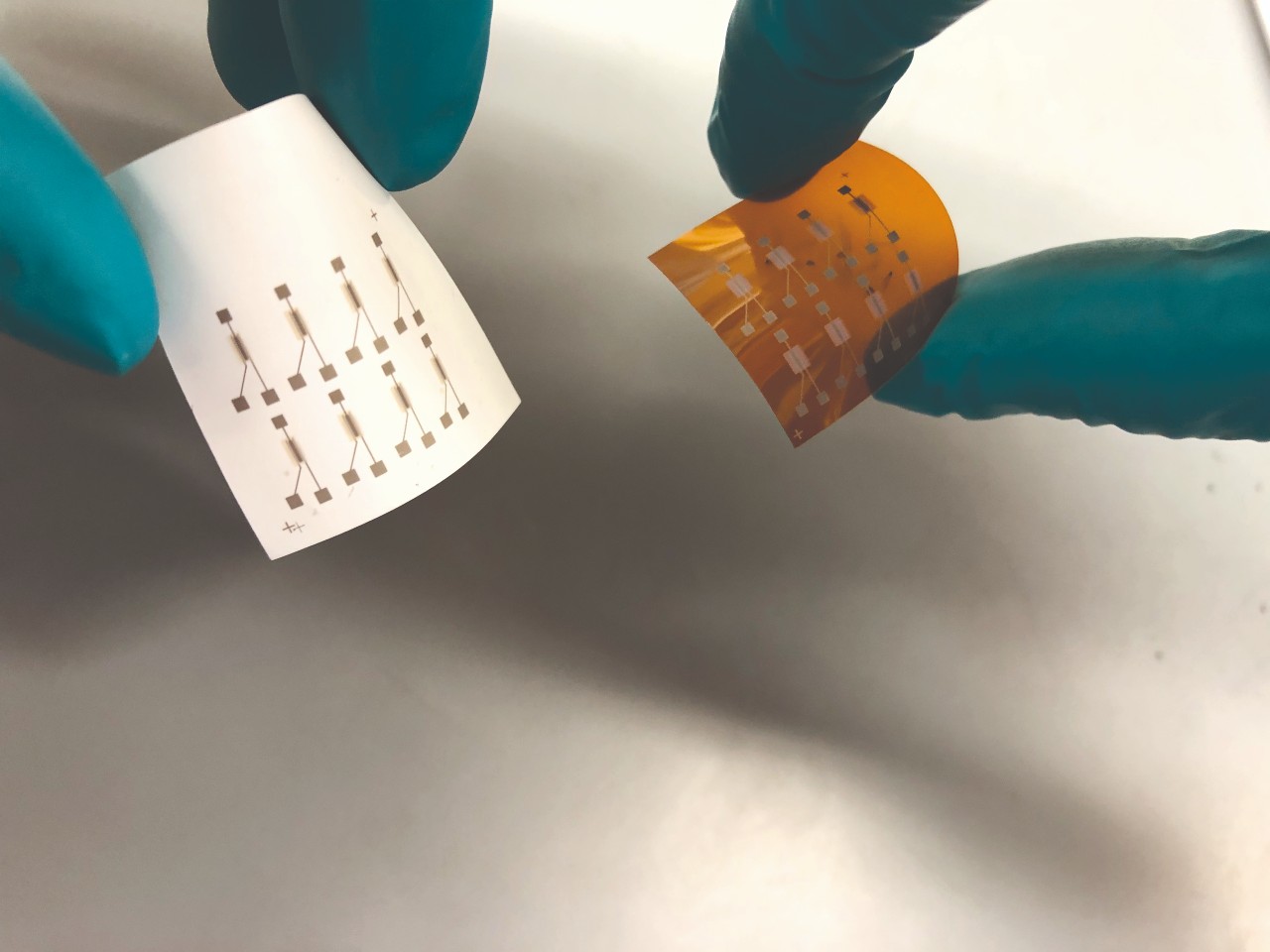
Using these 2D hexagonal boron nitride – or white graphene – inks, the team at Duke was able to print thin-film transistors using the platform it had developed for silver nanowires, semiconducting carbon nanotubes and other materials.
The white graphene offered an instant improvement on the inks that were already available, which are largely based on organic materials or metal oxides, and have a range of problems that inhibit their use in flexible printed circuits.
Often, they exhibit low carrier mobility or poor air stability, and they must be baked at high temperatures after the printing process, which rules out printing on certain substrates.

“Using our inks, Aaron was able to develop fully functional transistors,” Casiraghi says. “His philosophy is to make the device in the printer.
“Printing is usually just one step in the fabrication process, with some elements made in the printer before other processes take place. That method does not create devices straight out of the printer.
“Now we have taken a big step forward in realising Aaron’s vision.
“Boron nitride is a very good insulator and it is already used in graphene-based devices, where it proves to be very stable. We did not know if it would work in a transistor, though it has very good electrical properties at low temperatures.”
Thankfully, it did. It’s now possible to fully fabricate thin-film transistors with carbon nanotube channel regions with nothing more than the aerosol printer in Franklin’s lab.
The temperature of 80°C, which can be achieved in the printer itself, is the lowest reported temperature for the successful printing of a nanotube-based thin-film transistor on to flexible paper and plastic substrates.
“Our report shows that further research efforts could be developed with just the printer,” adds Franklin.
“Insulating inks are a big challenge that we haven’t fully solved yet, but we wanted to not bake it, so that we could achieve print-in-place transistors, and we have.”
The use of an aerosol printer was key to that success. Although it makes it possible to print functional circuits at relatively low temperatures, the process of delivering ink droplets to a substrate with micron-level accuracy needs to be precisely controlled, which demands an understanding of both aerosol physics and fluid mechanics.
“The tuning of printing parameters is important to ensure consistent behaviour and there are lots of parameters in an aerosol printer,” says Franklin.
“The droplets of ink are guided on to the circuit in an inert gas stream, so they are landing on a substrate like a drop of rain on concrete in the summer. It is chaotic, so the final properties are very sensitive to the printing process.”
The future for print-in-place electronics
Franklin’s vision goes beyond what he and Casiraghi have already achieved.
The team at Duke is now hoping to use the inks to deliver a print-in-place technique that is gentle enough for more delicate substrates, and Franklin sees an opportunity to develop ‘designer materials’ with customisable properties to suit the unique needs of specific applications.
Successful printing at 80ºC, without extra treatment outside the printer, is undoubtedly a big leap forward, but the ultimate goal is to deliver the same outcome at room temperature.
Once that is achievable, it will open up enticing possibilities in many fields, not least healthcare.
Ultimately, a customised circuit model for a wearable medical device could be uploaded to a database and printed as required in a local clinic or at a patient’s home, opening the door to personalised, decentralised health monitoring and treatment.
Patients could, for example, print a flexible, skin-mimicking device in their own home to track highly specific physiological data at minimal cost or discomfort.
The diagnostic potential could well help shift more health services from focusing on cures to enabling prevention. For now, reality is still playing catch-up, but print-in-place is undoubtedly the future of printable electronics.
This article first appeared in Medical Device Developments Vol. 2 2020. The full publication can be viewed online here.


